|
| |
Silicon (nano)photonic devices fabrication with 193nm and 248nm (DUV) Optical lithographyResearch Area:
Silicon Photonics Process Technology Main Researcher: Shankar Kumar Selvaraja
One major limitation for the widespread use of photonic crystals is the lack of efficient fabrication technologies. Most photonic crystals today are defined using e-beam lithography, a technique which can handle the resolutions required for photonic crystals at telecom wavelengths, but lacks the possibility for industrial application due to long writing times. Other techniques used for the large-scale fabrication of current PICs cannot print the fine details of photonic crystals.
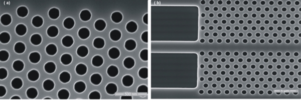
(a) Photonic crystals of 300nm pitch and 180nm hole dia and (b) W1 photonic crystal waveguide fabricated by 193nm lithography technology.
Deep UV lithography has the promise to solve this issue. This optical lithography technique based on excimer lasers with wavelength of 248nm and shorter is used state-of-the-art CMOS-facilities. The short wavelengths (193nm) can resolve periodic structures with periods down to a few 100nm.
Our material of choice is Silicon-on-Insulator. SOI is a good material system for the fabrication of Photonic Crystals because it is transparent for the main telecom wavelenghts, it has a high refractive index contrast, and it can be processed in silicon-based facilities.
As photonic crystal structures differ significantly from typical CMOS-circuits, lithography knowledge cannot be ported in a straightforward manner to photonic crystals. Key differences between these two types of structures are the lattice type (preferably triangular for photonic crystals versus square in CMOS-circuits) and the fill factor of the unit cell. We have therefore, studied the possibilities of manufacturing photonic crystal-like structures with this technology. For this purpose, we used the 248nm and 193nm deep UV lithography facilities available at IMEC. These consist of an ASML PAS 5500/750 and PAS 5500/1100 DUV stepper attached to an automated resist processing track.
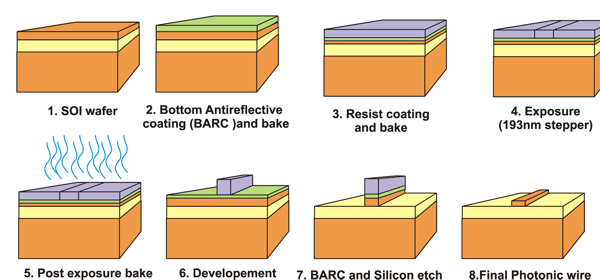
Fabrication process with 19nm deep UV lithography
For Photonic wires of 450nm wide fabricated using 193nm optical lithography and etch, we achieved a propagation loss of 2.8 dB/cm, which is the lowest wire loss reported using optical lithography. This loss is further reduced to 1.8 dB/cm by applying a surface treatment to the wires. For photonic crystal waveguides (with 248nm process), the losses are still an order of magnitude higher, with 7.5dB/mm for a W1 waveguide.
We have also implemented a large number of WDM-devices, such as Arrayed Waveguide gratings, planar curved gratings, coupled cavity waveguides, lattice filters and resonators.
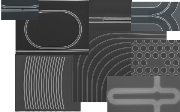
Photonic structures fabricated by 193nm lithography technology
Other people involved: Related Research Projects
Downloads  Fabrication of SOI Photonic Crystals with deep UV lithography
 Nanophotonic ICs: the promise and the problems (Norway 2004)
(Nano)photonics in Silicon(-on-Insulator)
Silicon-on-Insulator based Nanophotonics Why, How, What for?
PhD thesises -
Wim Bogaerts, Nanofotonische Golfgeleiders en Fotonische Kristallen in Silicium-op-Isolator, Nanophotonic Waveguides and Photonic Crystals in Silicon-on-Insulator, (4/2004)
-
Pieter Dumon, Ultra-compacte geïntegreerde optische filters in silicium-op-isolator op basis van waferschaaltechnologie, Ultra-Compact Integrated Optical Filters in Silicon-on-insulator by Means of Wafer-Scale Technology, (3/2007)
-
Joost Brouckaert, Integratie van fotodetectoren op siliciumgebaseerde fotonische circuits voor spectroscopische toepassingen, Integration of Photodetectors on Silicon Photonic Integrated Circuits (PICs) for Spectroscopic Applications, (10/2010)
-
Shankar Kumar Selvaraja, Fabricagetechnologieen op waferschaal voor fotonische geintegreerde circuits in silicium, Wafer-Scale Fabrication Technology for Silicon Photonic Integrated Circuits, (2/2011)
-
Thijs Spuesens, Compacte 'on-chip' optische interconnecties op silicium door heterogene integratie van III-V microbronnen en detectoren, Compact on-chip Optical Interconnects on Silicon by Heterogeneous Integration of III-V Microsources and Detectors, (3/2014)
Patents PublicationsInternational Journals
-
W. Xie, M. Fiers, S. Selvaraja, P. Bienstman, J. Van Campenhout, Philippe Absil, D. Van Thourhout,
High-Q Photonic Crystal Nanocavities on 300mm SOI Substrate Fabricated With 193 nm Immersion Lithography, Journal of Lightwave Technology, 32(18), p.1457 - 1462 doi:10.1109/JLT.2014.2308061 (2014) .
-
D.-X. Xu, J. H. Schmid, G. T. Reed, G. Z. Mashanovich, D. J. Thomson, M. Nedeljkovic, X. Chen, D. Van Thourhout, S. Keyvaninia, S. Selvaraja,
Silicon photonic integration platform – Have we found the sweet spot?, IEEE Journal of Selected Topics in Quantum Electronics (invited), 20(4), doi:10.1109/jstqe.2014.2299634 (2014) .
-
T. Spuesens, F. Mandorlo, P. Rojo-Romeo, P. Regreny, N. Olivier, J.M. Fedeli, D. Van Thourhout,
Compact integration of optical sources and detectors on SOI for optical interconnects fabricated in a 200 mm CMOS pilot line, Journal of Lightwave Technology, 30(11), p.1764-1770 doi:10.1109/jlt.2012.2189871 (2012) .
-
W. Bogaerts, S. Selvaraja,
Compact Single-mode Silicon Hybrid Rib/Strip Waveguide with Adiabatic Bends, IEEE Photonics Journal, 3(3), p.422-232 doi:10.1109/JPHOT.2011.2142931 (2011) .
-
W. Bogaerts, S. Selvaraja, P. Dumon, J. Brouckaert, K. De Vos, D. Van Thourhout, R. Baets,
Silicon-on-Insulator Spectral Filters Fabricated with CMOS Technology, J. Sel. Top. Quantum Electron. (invited), 16(1), p.33-44 doi:10.1109/JSTQE.2009.2039680 (2010) .
-
S. Selvaraja, W. Bogaerts, P. Dumon, D. Van Thourhout, R. Baets,
Sub-nanometer linewidth uniformity in silicon nano-photonic waveguide devices using CMOS fabrication technology , IEEE Journal on Selected Topics in Quantum Electronics, 16(1), p.316 - 324 doi:10.1109/JSTQE.2009.2026550 (2010) .
-
A. Kazmierczak, F. Dortu, D. Giannone, W. Bogaerts, E. Drouard, P. Rojo-Romeo, F. Gaffiot,
Synthesis of highly integrated optical network based on microdisk-resonator add-drop filters in SOI technology, Optical Engineering, 48(10), p.104601 doi:10.1117/1.3242841 (2009).
-
D. Neel, T. Benyattou, P. Sanchis, J. Marti, W. Bogaerts, P. Dumon, R. Baets,
Optical near-field study of photonic crystal tapers, Applied Optics, 48(30), p.5718-5721 doi:10.1364/AO.48.005718 (2009) .
-
J. Brouckaert, G. Roelkens, S. Selvaraja, W. Bogaerts, P. Dumon, S. Verstuyft, D. Van Thourhout, R. Baets,
Silicon-on-Insulator CWDM Power Monitor/Receiver with Integrated Thin Film InGaAs Photodetectors, IEEE Photonics Technology Letters, 21(19), p.1423 doi:10.1109/lpt.2009.2027999 (2009) .
-
S. Selvaraja, P. Jaenen, W. Bogaerts, P. Dumon, D. Van Thourhout, R. Baets,
Fabrication of Photonic Wire and Crystal Circuits in Silicon-on-Insulator Using 193nm Optical Lithography, Journal of Lightwave Technology, 27(18), p.4076-4083 doi:10.1109/JLT.2009.2022282 (2009) .
-
A. Kazmierczak, W. Bogaerts, E. Drouard, F. Dortu, P. Rojo-Romeo, F. Gaffiot, D. Van Thourhout, D. Giannone,
Highly Integrated Optical 4x4 Crossbar in Silicon-on-Insulator Technology, Journal of Lightwave Technology, 27(16), p.3317-3323 doi:10.1109/JLT.2008.2010462 (2009) .
-
J. Teng, P. Dumon, W. Bogaerts, H. Zhang, X. Jian, X. Han, M. Zhao, G. Morthier, R. Baets,
Athermal Silicon-on-insulator ring resonators by overlaying a polymer cladding on narrowed waveguides, Optics Express, 17(17), p.14627-14633 doi:10.1364/OE.17.014627 (2009) .
-
S. Selvaraja, Erik Sleeckx, Marc Schaekers, W. Bogaerts, D. Van Thourhout, P. Dumon, R. Baets,
Low-Loss Amorphous Silicon-On-Insulator Technology for Photonic Integrated Circuitry, Optics Communications, 282(9), p. 1767-1770 doi:10.1016/j.optcom.2009.01.021 (2009) .
-
Landobasa Y.M. Tobing, Desmond C.S. Lim, P. Dumon, R. Baets, Mee-Koy Chin,
Finesse enhancement in silicon-on-insulator two-ring resonator system, Applied Physics Letters, 92, p.101122 doi:10.1063/1.2894203 (2008) .
-
J. Schrauwen, D. Van Thourhout, R. Baets,
Trimming of silicon ring resonator by electron beam induced compaction and strain, Optics Express, 16(6), p.3738-3743 doi:10.1364/oe.16.003738 (2008) .
-
J. Brouckaert, W. Bogaerts, S. Selvaraja, P. Dumon, R. Baets, D. Van Thourhout,
Planar Concave Grating Demultiplexer with High Reflective Bragg Reflector Facets, Photonics Technology Letters, 20(4), p.309-311 doi:10.1109/lpt.2007.915585 (2008) .
-
W. Bogaerts, P. Dumon, D. Van Thourhout, R. Baets,
Low-Loss, Low-Crosstalk Crossings for SOI Nanophotonic Waveguides, Optics Letters, 32(19), p.2801-2803 doi:10.1364/OL.32.002801 (2007) .
-
J. Brouckaert, W. Bogaerts, P. Dumon, D. Van Thourhout, R. Baets,
Planar Concave Grating Demultiplexer Fabricated on a Nanophotonic Silicon-on-Insulator Platform, Journal of Lightwave Technology, 25(5), p.1269-1275 doi:10.1109/jlt.2007.893025 (2007) .
-
W. Bogaerts, D. Taillaert, P. Dumon, D. Van Thourhout, R. Baets,
A polarization-diversity wavelength duplexer circuit in silicon-on-insulator photonic wires, Optics Express, 15(4), p.1567-1578 doi:10.1364/oe.15.001567 (2007) .
-
W. Bogaerts, P. Dumon, D. Van Thourhout, D. Taillaert, P. Jaenen, J. Wouters, S. Beckx, R. Baets,
Compact Wavelength-Selective Functions in Silicon-on-Insulator Photonic Wires, J. Selected Topics in Quantum Electronics, 12(6), p.1394-1401 doi:10.1109/jstqe.2006.884088 (2006) .
-
W.C.L. Hopman, A.J.F. Hollinck, R.M. de Ridder, K.O. van der Werf, V. Subramamiam, W. Bogaerts,
Nano-mechanical tuning and imaging of a photonic crystal micro-cavity resonance, Optics Express, 14(19), p.8745-8752 doi:10.1364/oe.14.008745 (2006) .
-
T.K. Liang, L.R. Nunes, M. Tuschiya, K.S. Abedin, T. Miyazaki, D. Van Thourhout, W. Bogaerts, P. Dumon, R. Baets, H.K. Tsang,
High speed logic gate using two-photon absorption in Silicon waveguides, Optics Communications, 265(1), p.171-174 doi:10.1016/j.optcom.2006.03.031 (2006) .
-
P. Dumon, G.R.A. Priem, L.R. Nunes, W. Bogaerts, D. Van Thourhout, P. Bienstman, T.K. Liang, M. Tsuchiya, P. Jaenen, S. Beckx, J. Wouters, R. Baets,
Linear and nonlinear nanophotonic devices based on silicon-on-insulator wire waveguides, Japanese Journal of Applied Physics, 45(8B), p.6589-6602 doi:10.1143/jjap.45.6589 (2006) .
-
P. Dumon, W. Bogaerts, D. Van Thourhout, D. Taillaert, R. Baets, J. Wouters, S. Beckx, P. Jaenen,
Compact wavelength router based on a Silicon-on-insulator arrayed waveguide grating pigtailed to a fiber array, Optics Express, 14(2), p.664-669 doi:10.1364/opex.14.000664 (2006) .
-
P. Sanchis, J. Marti, W. Bogaerts, P. Dumon, D. Van Thourhout, R. Baets,
Experimental results on adiabatic coupling into SOI photonic Crystal coupled-cavity waveguides, Photonics Technology Letters, 17(6), p.1199-1201 doi:10.1109/lpt.2005.846621 (2005) .
-
H. Gersen, T.J. Karle, R.J.P. Engelen, W. Bogaerts, J.P. Korterik, N.F. van Hulst, T.F. Krauss, L. Kuipers,
Direct observation of Bloch harmonics and negative phase velocity in photonic crystal waveguides, Physics Review Letters, 94(12), p.123901 doi:10.1103/physrevlett.94.123901 (2005) .
-
H. Gersen, T.J. Karle, R.J.P. Engelen, W. Bogaerts, J.P. Korterik, N.F. van Hulst, T.F. Krauss, L. Kuipers,
Real space observation of ultraslow light in photonic crystal waveguides., Physics Review Letters, 94(7), p.073903 doi:10.1103/physrevlett.94.073903 (2005) .
-
P.I. Borel, L.H. Frandsen, A. Harpoeth, J.B. Leon, H. Liu, M. Kristensen, W. Bogaerts, P. Dumon, R. Baets, V. Wiaux, S. Beckx, J. Wouters,
Bandwidth engineering of photonic crystal waveguide bends, Electronics Letters, 40(20), p.1263-1264 doi:10.1049/el:20046206 (2004) .
-
P. Sanchis, J. Garcia, J. Marti, W. Bogaerts, P. Dumon, D. Taillaert, R. Baets, V. Wiaux, J. Wouters, S. Beckx,
Experimental demonstration of high coupling efficiency between wide ridge dielectric waveguides and single-mode photonic crystal waveguides , IEEE Photon. Technol. Lett., 16(10), p.2272-2274 doi:10.1109/lpt.2004.833915 (2004) .
-
W. Bogaerts, P. Dumon, D. Taillaert, V. Wiaux, S. Beckx, B. Luyssaert, J. Van Campenhout, D. Van Thourhout, R. Baets,
SOI Nanophotonic Waveguide Structures Fabricated with Deep UV Lithography , Photonics and Nanostructures: Fundamentals and Applications (invited), 2(2), p.81-86 doi:10.1016/j.photonics.2004.07.002 (2004) .
-
L.H. Frandsen, P.I. Borel, Y.X. Zhuang, A. Harpoeth, M. Thorhauge, M. Kristensen, W. Bogaerts, P. Dumon, R. Baets, V. Wiaux, S. Beckx, J. Wouters,
Ultra Low Loss 3 dB Photonic Crystal Waveguide Splitter , Optics Letters, 29(14), p.1623-1625 doi:10.1364/OL.29.001623 (2004) .
-
P. Dumon, W. Bogaerts, V. Wiaux, J. Wouters, S. Beckx, J. Van Campenhout, D. Taillaert, B. Luyssaert, P. Bienstman, D. Van Thourhout, R. Baets,
Low-loss SOI Photonic Wires and Ring Resonators Fabricated with Deep UV Lithography, IEEE Photonics Technology Letters, 16(5), p.1328-1330 doi:10.1109/lpt.2004.826025 (2004) .
-
W. Bogaerts, D. Taillaert, B. Luyssaert, P. Dumon, J. Van Campenhout, P. Bienstman, D. Van Thourhout, R. Baets, V. Wiaux, S. Beckx,
Basic structures for photonic integrated circuits in Silicon-on-insulator, Optics Express (invited), 12(8), p.1583-1591 doi:10.1364/OPEX.12.001583 (2004) .
-
W. Bogaerts, V. Wiaux, D. Taillaert, S. Beckx, B. Luyssaert, P. Bienstman, R. Baets,
Fabrication of Photonic Crystals in Silicon-on-Insulator Using 248-nm Deep UV Lithography, IEEE Journal on Selected Topics in Quantum Electronics, 8(4), p.928-934 doi:10.1109/jstqe.2002.800845 (2002) .
Book / Book Chapter
-
W. Bogaerts, L. Liu, G. Roelkens,
Technologies and Building Blocks for On-Chip Optical Interconnects, Integrated Optical Interconnect Architectures for Embedded Systems (invited), doi:10.1007/978-1-4419-6193-8_2 (2012).
International Conferences
-
S. Selvaraja, Luis Fernandez, M. Vanslembrouck, Jean-Luc Everaert, P. Dumon, J. Van Campenhout, W. Bogaerts, Philippe Absil,
Si photonic device uniformity improvement using wafer-scale location specific processing, IEEE Photonics Conference 2012 (IPC), United States, p.725-726 doi:10.1109/ipcon.2012.6358827 (2012) .
-
Peter Verheyen, Guy Lepage, J Van Campenhout, M. Pantouvaki, Philippe Absil, P. De Heyn, W. Bogaerts, P. Dumon, S. Selvaraja,
Co-integration of Ge detectors and Si modulators in an advanced Si photonics platform, SPIE Photonics Europe 2012, 8431, Belgium, p.paper 39 doi:10.1117/12.921747 (2012) .
-
S. Selvaraja, E.Rosseel, L.Fernandez, Martin Tabat, W. Bogaerts, J. Hautala, P. Absil,
SOI thickness uniformity improvement using wafer-scale corrective etching for silicon nano-photonic device, 16th Annual Symposium of the IEEE Photonics Benelux Chapter, Belgium, p.289-292 (2011) .
-
H. Yu, W. Bogaerts, K. Komorowska, J. Van Campenhout, P. Verheyen, P. Absil, R. Baets,
12.5 Gbit/s carrier-depletion based silicon Mach-Zehnder modulator with a 2 V driven voltage, 16th Annual Symposium of the IEEE Photonics Benelux Chapter, Belgium, p.93-96 (2011) .
-
W. Bogaerts,
Silicon Photonics, Rusnanotech Forum (invited), Russia, p.Th.J.2.1 (2011) .
-
S. Selvaraja, E.Rosseel, L.Fernandez, Martin Tabat, W. Bogaerts, J. Hautala, P. Absil,
SOI Thickness Uniformity Improvement using Corrective Etching for Silicon Nano-Photonic Device, 8th International Conference on Group IV Photonics, United Kingdom, p.71-73 doi:10.1109/group4.2011.6053719 (2011) .
-
W. Bogaerts, S. Selvaraja, H. Yu, T. Spuesens, P. Mechet, S. Stankovic, S. Keyvaninia, J. Van Campenhout, P. Absil, G. Roelkens, D. Van Thourhout, R. Baets,
A Silicon Photonics Platform with Heterogeneous III-V Integration, Integrated Photonics Research, Silicon and Nano-Photonics (IPR) (invited), Canada, p.IWC2 doi:10.1364/iprsn.2011.iwc2 (2011) .
-
W. Bogaerts, P. Absil, D. Van Thourhout, J. Van Campenhout, S. Selvaraja, P. Dumon, H. Yu, A. Masood, G. Roelkens, R. Baets,
Optical Interconnect Technologies based on Silicon Photonics, MRS Spring 2011 (invited), United States, p.O10.1 (2011) .
-
W. Bogaerts, S. Selvaraja, P. Dumon, P. Absil, D. Van Thourhout, R. Baets,
Photonic Integrated Circuits in Silicon-on-Insulator, IEEE SOI Conference (invited), United States, p.9.02 doi:10.1109/soi.2010.5641404 (2010) .
-
S. Selvaraja, W. Bogaerts, P. Absil, D. Van Thourhout, R. Baets,
Record Low-Loss Hybrid Rib/Wire Waveguides for Silicon Photonic Circuits , Group IV Photonics 2010 (PD), China, (2010) .
-
W. Bogaerts, R. Baets, G. Roelkens, D. Van Thourhout, p. Absil, S. Selvaraja, H. Yu, A. Masood,
A silicon photonics platform with heterogeneous III-V integration, Workshop on the Future of Silicon Photonics (invited), China, p.11 (2010) .
-
S. Selvaraja, K. De Vos, W. Bogaerts, P. Bienstman, D. Van Thourhout, R. Baets,
Effect of Device Density on the Uniformity of Silicon Nano-Photonic Waveguide Devices, The 22nd Annual Meeting of the IEEE Photonics Society, Turkey, p.311-312 doi:10.1109/leos.2009.5343250 (2009) .
-
W. Bogaerts, P. Dumon, S. Selvaraja, D. Van Thourhout, R. Baets,
Silicon nanophotonic waveguide components, Silicon Nanoelectronics and Photonics (SiNEP) 2009 (invited), Spain, p.33-34 (2009) .
-
T. Vallaitis, D. Hillerkuss, J.-S. Li, R. Bonk, N. Lindenmann, P. Dumon, R. Baets, M.L. Scimeca, I. Biaggio, F. Diederich, C. Koos, W. Freude, J. Leuthold,
All-Optical Wavelength Conversion Using Cross-Phase Modulation at 42.7 Gbit/s in Silicon-Organic Hybrid (SOH) Waveguides, Photonics in Switching 2009, Italy, doi:10.1109/ps.2009.5307823 (2009) .
-
S. Clemmen, K. Phan Huy, W. Bogaerts, R. Baets, P. Emplit, S. Massar,
Towards an Integrated Narrowband Source for Quantum Information: Photon Pair Generation in a Silicon Racetrack Resonator, Integrated Photonics and Nanophotonics Research and Applications (IPNRA), United States, p.IME1 doi:10.1364/ipnra.2009.ime1 (2009) .
-
S. Selvaraja, D. Vermeulen, Marc Schaekers, Erik Sleeckx, W. Bogaerts, G. Roelkens, P. Dumon, D. Van Thourhout, R. Baets,
Highly Efficient Grating Coupler between Optical Fiber and Silicon Photonic Circuit, Conference on Lasers and Electro-Optics (CLEO) 2009 , United States, p.CTuC6 doi:10.1364/cleo.2009.ctuc6 (2009) .
-
D. Van Thourhout, I. O'Connor, A. Scandurra, L. Liu, W. Bogaerts, S. Selvaraja, G. Roelkens,
Nanophotonic Devices for Optical Networks-on-Chip, Conference on Lasers and Electro-Optics (CLEO) (invited), United States, p.CMAA2 doi:10.1364/cleo.2009.cmaa2 (2009) .
-
S. Selvaraja, W. Bogaerts, P. Dumon, D. Van Thourhout, R. Baets,
Amorphous silicon photonic crystals made with 193nm lithography, The 8th International Photonic & Electromagnetic Crystal Structures Meeting (PECS), Australia, (2009) .
-
S. Selvaraja, P. Dumon, W. Bogaerts, D. Van Thourhout, R. Baets, E. Sleeckx, M. Schaekers,
Demonstration Of Optical Via And Low-Loss Optical Crossing For Vertical Integration Of Silicon Photonic Circuit, PHOTONICS 2008:The International Conference on Fiber Optics and Photonics (BEST PAPER AWARD), India, (2008) .
-
S. Clemmen, K.P. Huy, W. Bogaerts, R. Baets, P. Emplit, S. Massar,
Photon pair generation in a continuous regim in nanophotonic silico waveguides, 13th Annual Symposium of the IEEE/LEOS Benelux Chapter, Netherlands, p.67-70 (2008) .
-
J. Brouckaert, S. Selvaraja, W. Bogaerts, G. Roelkens, M.Y. Ling, J. Allaert, P. Dumon, D. Van Thourhout, R. Baets,
Silicon-on-Insulator Microspectrometer, 13th Annual Symposium of the IEEE/LEOS Benelux chapter, Netherlands, p.7-10 (2008) .
-
J. Brouckaert, G. Roelkens, S. Selvaraja, W. Bogaerts, P. Dumon, S. Verstuyft, Z. Yu, D. Van Thourhout, R. Baets,
Miniature Integrated Spectrometer Fabricated on a Silicon-on-Insulator Substrate, Leos Annual Meeting, United States, p.MF3 doi:10.1109/leos.2008.4688485 (2008) .
-
J. Brouckaert, G. Roelkens, S. Selvaraja, W. Bogaerts, P. Dumon, S. Verstuyft, D. Van Thourhout, R. Baets,
Compact Silicon-on-Insulator Wavelength Demultiplexer with Heterogeneously Integrated InAlAs/InGaAs Photodetectors, ECOC 2008, Belgium, p.Tu.4.C.5 doi:10.1109/ecoc.2008.4729247 (2008) .
-
J. Schrauwen, D. Van Thourhout, R. Baets,
Trimming of silicon ring resonator by electron beam induced compaction, ECIO 2008, (2008) .
-
S. Selvaraja, W. Bogaerts, D. Van Thourhout, R. Baets,
Fabrication of Uniform Photonic Devices Using 193nm Optical Lithography in Silicon-on-Insulator , 14th European Conference on Integrated Optics (ECIO), Netherlands, (2008) .
-
S. Selvaraja, D. Van Thourhout, R. Baets,
Fabrication of photonic integrated circuits using high resolution CMOS fabrication process, ePIXnet Springshool 2008, Italy, (2008) .
-
P. Dumon, J.-M. Fédéli, W. Bogaerts,
The ePIXnet silicon photonics platform, Workshop on Fibers and Optical Passive Components (invited), Taiwan, p.W4B-1 doi:10.1109/group4.2007.4347696 (2007) .
-
S. Selvaraja, P. Jaenen, S. Beckx, W. Bogaerts, P. Dumon, D. Van Thourhout, R. Baets,
Silicon nanophotonic wire structures fabricated by 193nm optical lithography , LEOS Annual Meeting 2007 (invited), United States, doi:10.1109/leos.2007.4382268 (2007) .
-
W. Bogaerts, P. Dumon, J.-M. Fedeli, A. Tchelnokov, D. Van Thourhout, S. Selvaraja, R. Baets,
A Platform for Silicon-on-Insulator Nanophotonics on Industrial CMOS Tools, Photonic and Electromagnetic Crystal Structures (PCS-VII), United States, (2007) .
-
R. Baets, W. Bogaerts, D. Taillaert, P. Dumon, D. Van Thourhout,
SOI Photonic Wire Based Components with Compact and Efficient Fiber Couplers , Optical Fiber Communications (invited), United States, p.OWG3 doi:10.1109/ofc.2007.4348871 (2007) .
-
F. Van Laere, W. Bogaerts, D. Taillaert, P. Dumon, D. Van Thourhout, R. Baets,
Compact Focusing Grating Couplers Between Optical Fibers and Silicon-on-Insulator Photonic Wire Waveguides , Optical Fiber Communications, United States, p.OWG1 doi:10.1109/ofc.2007.4348869 (2007) .
-
W. Bogaerts, D. Taillaert, P. Dumon, E. Pluk, D. Van Thourhout, R. Baets,
A Compact Polarization-Independent Wavelength Duplexer Using a Polarization-Diversity SOI Photonic Wire Circuit , Optical Fiber Communications, United States, p.OTuM2 doi:10.1109/ofc.2007.4348826 (2007) .
-
W. Bogaerts, P. Dumon, D. Van Thourhout, R. Baets,
Compact, Low-Loss Waveguide Crossings for High-Index-Contrast SOI Photonic Wires , Optical Fiber Communications, United States, p.OTuM1 doi:10.1109/ofc.2007.4348825 (2007) .
-
E.D. Kyriakis-Bitzaros, E. Grivas, G. Halkias, S. Katsafouros, P. Dumon, G. Morthier, R. Baets, T. Farell, N. Ryan, I. McKenzie, E. Armadillo,
A WDM Optical Backplane with AWG Based Passive Routing, Photonics in Switching 2006, Greece, p.273-275 doi:10.1109/ps.2006.4350206 (2006) .
-
D. Néel, T. Benyattou, P. Sanchis, J. Marti, W. Bogaerts, P. Dumon, D. Van Thourhout, R. Baets,
Near-Field Characterization of Coupled-Cavity Waveguides on SOI, European Conference on Optical Communication (ECOC) 2006, France, p.Th3.1.2 doi:10.1109/ecoc.2006.4800986 (2006) .
-
D. Néel, T. Benyattou, P. Sanchis, J. Marti, W. Bogaerts, P. Dumon, R. Baets,
Characterization of SOI photonic crystals tapers by Scanning Near-Field Optical Microscopy (SNOM), European Materials Research Society (E-MRS) Spring Meeting, France, p.D S4 04 (2006) .
-
P. Dumon, W. Bogaerts, D. Van Thourhout, G. Morthier, R. Baets,
Compact arrayed waveguide grating devices in silicon-on-insulator, Proceedings Symposium IEEE/LEOS Benelux Chapter, Belgium, p.105-108 (2005) .
-
W. Bogaerts, P. Dumon, J. Wouters, P. Jaenen, S. Beckx, V. Wiaux, D. Van Thourhout, D. Taillaert, B. Luyssaert, R. Baets,
Silicon-on-Insulator Nanophotonics, SPIE Optics and Optoelectronics (invited), 5956, Poland, p.5956R-1-15 (2005) .
-
R. Baets, D. Van Thourhout, G. Morthier, W. Bogaerts, L. Vanholme,
Silicon-on-insulator based high index contrast waveguide devices: research in europe, 11th Microoptics Conference (MOC) (invited), Japan, p.E2, Session C ( 4 pages) (2005) .
-
G. Roelkens, P. Dumon, W. Bogaerts, D. Van Thourhout, R. Baets,
Efficient fiber to SOI photonic wire coupler fabricated using standard CMOS technology, Proceedings of the 18th Annual Meeting of the IEEE Lasers & Electro-Optics Society (LEOS 2005), Australia, p.TuD2 doi:10.1109/leos.2005.1547946 (2005) .
-
T.K. Liang, L.R. Nunes, M. Tsuchiya, H.K. Tsang, D. Van Thourhout, P. Dumon, R. Baets, W. Bogaerts,
All-optical Wavelength Conversion in Silicon Wire Waveguides, European Conference on Optical Communication (ECOC) 2005, United Kingdom, p.We4.P.043 doi:10.1049/cp:20050622 (2005) .
-
P. Sanchis, J. Marti, W. Bogaerts, P. Dumon, R. Baets,
Experimental Results and 3D Analysis of a High Efficiency Coupling Technique for Planar Photonic Crystals, European Conference on Optical Communication (ECOC) 2005, United Kingdom, p.Tu1.6.4 doi:10.1049/cp:20050433 (2005) .
-
R. Baets, P. Dumon, W. Bogaerts, G. Roelkens, D. Taillaert, B. Luyssaert, G.R.A. Priem, G. Morthier, P. Bienstman, D. Van Thourhout,
Silicon-on-insulator based Nano-photonics: Why, How, What for?, Group IV Photonics (invited), Belgium, p.168-170 (2005) .
-
L.R. Nunes, T.K. Liang, M. Tsuchiya, D. Van Thourhout, P. Dumon, R. Baets,
Ultrafast Non-inverting Wavelength Conversion by Cross-Absorption Modulation in Silicon Wire Waveguides, Group IV Photonics, Belgium, p.156-158 doi:10.1109/group4.2005.1516436 (2005) .
-
P. Dumon, R. Baets, R. Kappeler, D. Barros, I. McKenzie, D. Doyle,
Measured radiation sensitivity of Silica-on-Silicon and Silicon-on-insulator micro-photonic devices for potential space application, Optics and Photonics, Photonics for Space Environments X, 5897, United States, doi:10.1117/12.617024 (2005) .
-
D. Taillaert, R. Baets, P. Dumon, W. Bogaerts, D. Van Thourhout, B. Luyssaert, V. Wiaux, S. Beckx, J. Wouters,
Silicon-on-Insulator Platform for Integrated Wavelength-Selective Components, Workshop on Fibres and Optical Passive Components (invited), Italy, doi:10.1109/wfopc.2005.1462110 (2005) .
-
D. Néel, T. Benyattou, R. Orobtchouk, P. Dumon, D. Van Thourhout,
SNOM for the optical characterisation of photonic crystal structures, Workshop on Photonic and Electromagnetic Crystal Structures (PECS-VI), Greece, p.C.32 (2005) .
-
T.J. Karle, T.F. Krauss, W. Bogaerts, H. Gersen, R.J.P. Engelen, J.P. Korterik, N.F. van Hulst, L. Kuipers,
Slow light, modal dispersion and mini stop bands in photonic crystal waveguides: experiments and modelling, Workshop on Photonic and Electromagnetic Crystal Structures (PECS-VI), Greece, p.B.40 (2005) .
-
P. Sanchis, A. Martinez, J. Garcia, F. Cuesta-Soto, J. Marti, P. Dumon, W. Bogaerts, D. Van Thourhout, R. Baets,
Experimental demonstration of adiabatic coupling into SOI photonic crystal coupled-cavity waveguides, Conference on Lasers and Electro-Optics/Quantum Electronics and Laser Science Conference/Photonic Applications, Systems and Technologies Conference (CLEO/QELS 2005), United States, p.CTuDD2 doi:10.1109/cleo.2005.202057 (2005) .
-
P. Dumon, W. Bogaerts, D. Van Thourhout, D. Taillaert, V. Wiaux, S. Beckx, J. Wouters, R. Baets,
Wavelength-selective components in SOI photonic wires fabricated with deep UV lithography, Group IV Photonics, Hong Kong, p.WB5 doi:10.1109/group4.2004.1416642 (2004) .
-
P. Dumon, W. Bogaerts, D. Van Thourhout, D. Taillaert, V. Wiaux, S. Beckx, J. Wouters, R. Baets,
Cascaded Mach-Zehnder Filters in Silicon-on-Insulator Photonic Wires fabricated with deep UV lithography, European Conference on Optical Communication (ECOC) 2004, Th.(Post-deadline), Sweden, p.24-25 (2004) .
-
B. Luyssaert, P. Vandersteegen, W. Bogaerts, P. Dumon, P. Sanchis, J. Marti, R. Baets,
A Versatile Optical Spot-Size Converter Design, European Conference on Optical Communication (ECOC) 2004, We(3), Sweden, p.468-469 (2004) .
-
R. Baets,
Photonic Crystal Research in IST, European Conference on Optical Communication (ECOC) 2004 (invited), 5(Symposia), Sweden, p.80-82 (2004) .
-
M. Thorhauge, L.H. Frandsen, P.I. Borel, A. Harpoeth, Y.X. Zhuang, M. Kristensen, W. Bogaerts, P. Dumon, R. Baets, V. Wiaux, J. Wouters, S. Beckx,
Novel low-loss 60° bends in photonic crystal waveguides, CLEO/IQEC, United States, p.CWP2 (2004).
-
R. Baets, W. Bogaerts,
Nanophotonic waveguides in SOI by means of deep UV lithography, Photonic and Electromagnetic Crystal Structures (PECS-V) (invited), Japan, p.160 (2004) .
-
B. Luyssaert, P. Vandersteegen, W. Bogaerts, V. Wiaux, J. Wouters, S. Beckx, R. Baets,
Compact Photonic Spot-Size Converter, Photonic and Electromagnetic Crystal Structures (PECS-V), Japan, p.193 (2004).
-
P. Sanchis, J. Garcia, F. Cuesta-Costo, A. Martinez, J. Blasco, J. Marti, W. Bogaerts, P. Dumon, D. Taillaert, R. Baets,
Experimental demonstration of a high efficiency coupling technique for planar photonic crystal circuits, Photonic and Electromagnetic Crystal Structures (PECS-V), Japan, p.128 (2004).
-
M. Kristensen, L.H. Frandsen, A. Harpoeth, Y.X. Zhuang, P.I. Borel, W. Bogaerts, P. Dumon, R. Baets, V. Wiaux, J. Wouters, S. Beckx,
Large bandwidth 60° bend in photonic crystal waveguides, Photonic and Electromagnetic Crystal Structures (PECS-V), Japan, p.93 (2004).
-
L.H. Frandsen, P.I. Borel, A. Harpoeth, M. Kristensen, M. Thorhauge, W. Bogaerts, P. Dumon, R. Baets, V. Wiaux, J. Wouters, S. Beckx,
Ultra low loss photonic crystal waveguide 3 dB splitter, Photonic and Electromagnetic Crystal Structures (PECS-V), Japan, p.146 (2004).
-
Y.X. Zhuang, L.H. Frandsen, A. Harpøth, M. Thorhauge, M. Kristensen, P.I. Borel, W. Bogaerts, R. Baets,
Wavelength tuning of photonic crystal waveguides fabricated using 248-nm deep UV lithography , OFC 2004, United States, p.ThR2 (2004).
-
P. Dumon, W. Bogaerts, J. Van Campenhout, V. Wiaux, J. Wouters, S. Beckx, R. Baets,
Low-loss photonic wires and compact ring resonators in silicon-on-insulator, LEOS Benelux Annual Symposium 2003, Netherlands, (2003) .
-
P. Dumon, W. Bogaerts, J. Van Campenhout, V. Wiaux, J. Wouters, S. Beckx, R. Baets,
Low-loss, single-mode photonic wires ring resonators in Silicon-on-Insulator, LEOS 2003, 1, United States, p.289-299 doi:10.1109/leos.2003.1251751 (2003) .
-
W. Bogaerts, P. Dumon, V. Wiaux, J. Wouters, S. Beckx, R. Baets,
Tolerance control for photonic crystal structures fabricated with deep UV lithography, ECOC 2003, 5, Italy, p.46-47 (2003) .
-
W. Bogaerts, V. Wiaux, P. Dumon, D. Taillaert, J. Wouters, S. Beckx, J. Van Campenhout, B. Luyssaert, D. Van Thourhout, R. Baets,
Large-scale production techniques for photonic nanostructures, Proc. SPIE (invited), 5225, United States, p.101-112 doi:10.1117/12.503665 (2003) .
-
R. Baets, P. Bienstman, W. Bogaerts, D. Taillaert, B. Luyssaert,
Coupling issues in strongly confined nanophotonic waveguides, ICTON 2003 (invited), Poland, p.191-192 doi:10.1109/icton.2003.1264613 (2003) .
-
T.F. Krauss, R. Wilson, R. Baets, W. Bogaerts, M. Kristensen, P.I. Borel, L.H. Frandsen, M. Thorhauge, B. Tromborg, A. Lavrinenko, R.M. De La Rue, H. Chong, L. Socci, M. Midrio, D. Gallagher,
Photonic Integrated Circuits using Crystal Optics (PICCO), European Conference on Integrated Optics (ECIO) (invited), Czech Republic, p.113-117 (2003) .
-
W. Bogaerts, V. Wiaux, D. Taillaert, S. Beckx, R. Baets,
SOI Photonic Crystal components fabricated with deep UV lithography, PECS-IV, United States, p.40 (2002) .
-
W. Bogaerts, V. Wiaux, D. Taillaert, S. Beckx, R. Baets,
Photonic Crystal Waveguides in SOI fabricated with deep UV lithography, European Conference on Optical Communication ECOC 2002, Denmark, p.4.4.5 (2002) .
-
W. Bogaerts, D. Taillaert, R. Baets, V. Wiaux, S. Beckx,
Large-scale production techniques for photonic nanostructures using excimer laser replication, Integrated Photonics Research (IPR) (invited), Canada, doi:10.1364/ipr.2002.ifh4 (2002) .
-
W. Bogaerts, V. Wiaux, D. Taillaert, S. Beckx, R. Baets,
Fabrication of Ultra-Compact Photonic Structures in Silicon-on-Insulator (SOI) Using 248 nm Deep UV Lithography, International Conference on Transparent Optical Networks (ICTON) 2002, 2, Poland, p.30-33 doi:10.1109/icton.2002.1007842 (2002) .
-
W. Bogaerts,
SOI Photonic Crystal Fabrication Using Deep UV, NKT Summer School, Denmark, (2001).
-
W. Bogaerts, D. Taillaert, R. Baets, V. Wiaux, S. Beckx, M. Maenhoudt, G. Vandenberghe,
SOI Photonic Crystal Fabrication Using Deep UV Lithography, PECS III, United Kingdom, (2001) .
National Conferences
-
S. Selvaraja, R. Baets, D. Van Thourhout,
Nanophotonic integrated chip fabricated by CMOS technology, 8th FirW PhD Symposium, Belgium, (2007) .
-
P. Dumon, W. Bogaerts, D. Van Thourhout, R. Baets, P. Jaenen, S. Beckx, J. Wouters,
A nanophotonic 4x4 wavelength router in silicon-on-insulator, 6th UGent-FirW Doctoraatssymposium, Belgium, p.38 (paper nr. 27) (2005) .
-
P. Dumon, W. Bogaerts, D. Van Thourhout, V. Wiaux, J. Wouters, S. Beckx, R. Baets,
WDM filters in Silicon-on-insulator photonic wires, Doctoraatssymposium Faculteit Toegepaste Wetenschappen, Belgium, (2004) .
-
W. Bogaerts, P. Dumon, V. Wiaux, J. Wouters, S. Beckx, D. Taillaert, B. Luyssaert, J. Van Campenhout, D. Van Thourhout, R. Baets,
Nanophotonic waveguides in Silicon-on-Insulator Fabricated with CMOS Technology, 1st Flanders Engineering PhD Symposium, Belgium, p.63 (2003) .
-
B. Luyssaert, P. Vandersteegen, R. Baets,
Compact Photonic Spot-Size Converters, FTW PhD symposium, Belgium, p.57 (2003) .
-
W. Bogaerts, V. Wiaux, D. Taillaert, S. Beckx, R. Baets,
Making lots of little holes (Or using CMOS mass fabrication technology to make photonic crystals), LEOS benelux Photonic Crystal Workshop, Belgium, (2002).
Back to overview
|