The Master of Science in Silicon Photonics is a unique program that addresses a critical need for skilled professionals in the rapidly growing field of
integrated photonics.
With the combination of academic excellence, practical industry experience and flexible study formats, the program aims to train a new generation of engineers and researchers to drive innovation in silicon photonics.
The program provides students with a comprehensive and
cutting-edge curriculum, integrating theoretical knowledge with
hands-on experience in state-of-the-art laboratories.
Our commitment is to empower students with the skills and insights needed to address the complex challenges of this fast-evolving
and rapidly growing field. This way, our master program aims
for a large impact by developing a highly skilled workforce in
Silicon Photonics, educate students who can define new and
multidisciplinary directions in PIC research, and who can
function in international and multidisciplinary teams,
communicating with all relevant stakeholders.
What is Silicon Photonics?
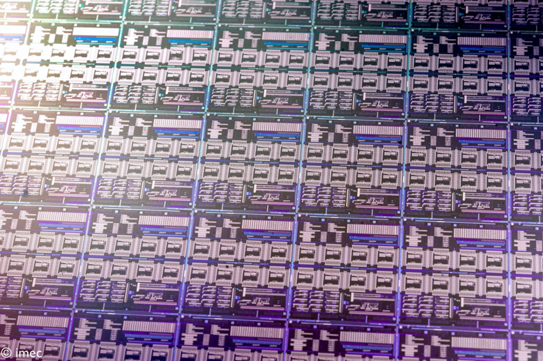
Silicon photonics is a subdomain of photonic integrated circuits (PICs), or “photonics on a chip”;
it is a technology that uses silicon-based materials to manipulate
and transmit light signals. It allows the creation of photonic circuits on a
silicon chip, integrating optical and electronic components. The key differentiator of silicon photonics is that the choice of materials allows the fabrication of photonic chips in the same facilities as CMOS
(complementary metal-oxide-semiconductor)
electronics, leveraging the decades of technology development in microelectronics. This opens a path to large-volume and low-cost manufacturing. The functionality of silicon PICs is defined by diverse opto-electronic elements such as modulators, optical amplifiers, laser sources, and detectors, connected into circuits by optical waveguides.
Applications include optical computing, optical interconnects, and data center communication systems where light is used to transmit data instead of electricity, allowing for much faster and more efficient data transfer.
It can also be used in sensing and healthcare applications to create compact, low-cost optical sensors that are capable of detecting minute changes in the environment.
Furthermore, it is also being explored for its potential to enable quantum computing, which relies on the manipulation of photons as information carriers.
Why do we offer this Master?
In order to address the labor shortage:
- in academia
there is a steady growing number of PhD positions in Integrated (silicon) Photonics at UGent, EU, worldwide - in industry
there is a booming demand for people with these skills at imec, within the PhotonDelta ecosystemEindhoven, at our local UGent spin-offs, and at many companies worldwide…
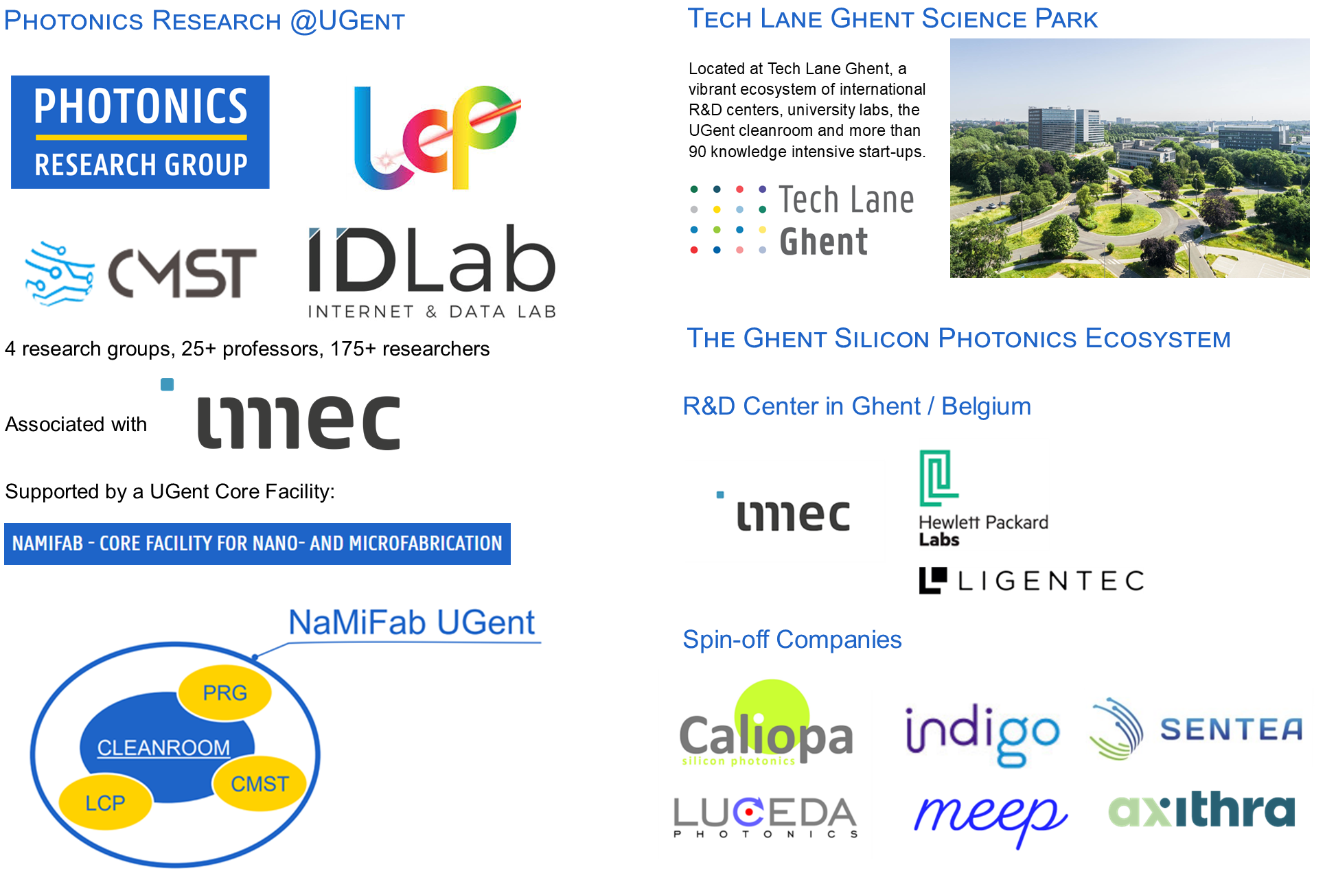
Why should UGent offer this Master?
Taking into account the full ecosystem, UGent should be among the best places in the world to study “Silicon Photonics” :
- Silicon Photonics expertise of the Photonics Research Group (9 ERC Grants, 7 ERC POCs, over 80 EU funded projects)
- Photonic Materials expertise at Liquid Crystals and Photonics research group
- Photonic Packaging at CMST (Centre for Microsystem Technology)
- Electronic-optical integration at IDLab Design
- Close connection/interaction/links to and with imec, spinoffs, R&D centers, industry … and an in-house accessible cleanroom