|
| |
III-V on silicon electroabsorption modulatorsResearch Area:
Heterogeneous integration technology for silicon photonics ,
Silicon photonics for telecom, datacom and interconnect Main Researcher: Martijn Tassaert
Although several types of modulators have been demonstrated on the silicon-on-insulator platform, the performance of these devices is no match to the intrinsically higher performance of III-V based electro-absorption modulators (EAM). Electro-absorption modulation in III-Vs is based on the quantum confined stark effect in a multi quantum well active region. This physical effect describes the band gap shrinking in a quantum well in a high electric field (see figure 1). This can be used for modulation, by using a carrier beam with a photon energy which is slightly lower than the quantum well band gap energy. Therefore, at zero bias absorption is quite low. By applying a reverse bias, a high electric field is created in the active region causing a band gap shrinkage, and hence dramatically increasing the absorption of the carrier beam. In this way, high speed modulation with a large extinction ratio can be achieved. By heterogeneously integrating III-Vs, this high performance can be brought to the silicon-on-insulator platform.
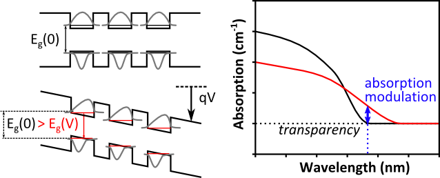
figure 1: quantum confined stark effect in multi quantum well structures. Left: effect of a high electric field on the band diagram. Right: resulting effect on the device absorption.
However, instead of just copying an existing modulator design used in III-V technology, the design can be improved by leveraging the high index contrast between the bonded III-V and surrounding DVS-BCB/oxide cladding. By optimizing the waveguide structure, the optical confinement in the active region can be maximized. In figure 2, an example waveguide structure is shown which allows a very high confinement in the active region. This allows more compact devices without loss of performance, and hence the device capacitance can be reduced. This lower capacitance can then be harnessed to either reach higher modulation speeds, as the bandwidth of an EAM is RC limited, or to reduce the operating voltage of the modulators by using a thinner active region.
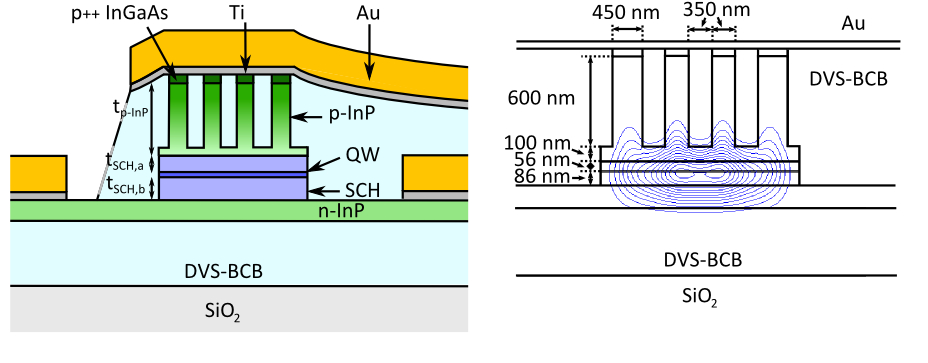
figure 2: gallery waveguide structure. The etched trenches in the top p-InP contact layer push the mode down, boosting the confinement in the active region.
Other people involved: PublicationsInternational Journals
-
A. Rahim, A. Hermans, B. Wohlfeil, D. Petousi, B. Kuyken, D. Van Thourhout, R. Baets,
Taking Silicon Photonics Modulators to a Higher Performance Level: State of the Art and A Review of New Technologies, Advanced Photonics (invited), 3(2), p. 024003-1 to 024003-23 doi:10.1117/1.AP.3.2.024003 (2021)
 . . -
M. Shahin, J. Rahimi Vaskasi, J. Van Kerrebrouck, P. Ossieur, X. Yin, J. Bauwelinck, G. Roelkens, G. Morthier,
80 Gbps NRZ-OOK Electro-Absorption Modulation of InP-on-Si DFB Laser Diodes, IEEE Photonics Technology Letters, 31(7), p.533-536 doi:10.1109/lpt.2019.2900518 (2019).
-
J. van Engelen, L. Shen, G. Roelkens, Y. Jiao, M. Smit, J. van der Tol,
A novel broadband electro-absorption modulator based on landfilling in n-InGaAs: design and simulations, Journal of Selected Topics in Quantum Electronics, 24(1), p.3300108 (8 pages) doi:10.1109/jstqe.2017.2765459 (2018) .
-
S. Dhoore, S. Uvin, D. Van Thourhout, G. Morthier, G. Roelkens,
Novel adiabatic tapered couplers for active III-V/SOI devices fabricated through transfer printing, Optics Express, 24(12), United States, p.12976-12990 doi:10.1364/OE.24.012976 (2016) .
-
Kaixuan Chen, Q. Huang, Jianhao Zhang, Jianxin Cheng, X. Fu, Chenzhao Zhang, Keqi Ma, Yaocheng Shi, D. Van Thourhout, G. Roelkens, L. Liu, Sailing He,
Wavelength-multiplexed duplex transceiver based on IIIV/Si hybrid integration for off-chip and on-chip optical interconnects, IEEE Photonics Journal, 8(1), p.7900910 doi:10.1109/jphot.2016.2516903 (2016) .
International Conferences
-
T. Reep, M. Billet, D. Van Thourhout, B. Kuyken,
Characterisation of a transfer-printed InP saturable absorber on a silicon platform, accepted for publication in Conference on Lasers and Electro-Optics Pacific Rim, South Korea, (to be published).
-
J. Zhang, L. Bogaert, M. Billet, D. Wang, B. Pan, S. Qin, E. Soltanian, S. Cuyvers, D. Maes, T. Vanackere, T. Vandekerckhove, S. Poelman, M. Kiewiet, I. Luntadila Lufungula, X. Guo, H. Li, J. De Witte, G. Lepage, P. Verheyen, J. Van Campenhout, B. Kuyken, G. Morthier, D. Van Thourhout, R. Baets, G. Roelkens,
Photonic integrated circuits realized using micro-transfer printing, PIERS (invited), (2023).
-
A. Abbasi, B. Moeneclaey, J. Verbist, X. Yin, J. Bauwelinck, G. Roelkens, G. Morthier,
56 Gb/s Electro-Absorption Modulation of a Heterogeneously Integrated InP-on-Si DFB Laser Diode, Optical Fiber Communication Conference (OFC), United States, p.paper Th4G.2 (3 pages) doi:10.1364/ofc.2017.th4g.2 (2017).
-
Z. Wang, M. Pantouvaki, G. Morthier, C. Merckling, J. Van Campenhout, D. Van Thourhout, G. Roelkens,
Heterogeneous Integration of InP Devices on Silicon, the 28th International Conference on Indium Phosphide and Related Materials (IPRM) (invited), Japan, p.paper ThD1-1 (2016) .
Back to overview
|