|
| |
III-V on silicon bonding technologyMain Researcher: Shahram Keyvaninia
Silicon photonics, based on the silicon-on-insulator (SOI) material platform, is emerging as an important platform for the realization of high-speed optical transceivers. Moreover, standard complementary metal oxide semiconductor (CMOS) processing infrastructure can be used to process these optical components. This allows high-yield fabrication and a reduction of the component cost through economies of scale. However, the fabrication of efficient light sources in silicon photonics is challenging due to silicon’s indirect bandgap. In order to create photonic integrated circuits comprising both opto-electronic and passive optical components, the heterogeneous integration of passive silicon-on-insulator waveguide circuits and active InP/InGaAsP components has been proposed, for applications in the telecommunication wavelength range.
Semiconductor wafer bonding allows the integration of high-quality III-V epitaxial layers on top of the silicon platform by transferring the III-V layer stack from its original growth substrate to the SOI wafer. Full wafer bonding, multiple die-to-wafer bonding or single die bonding can be envisaged, depending on the application. In all cases, an unprocessed III-V semiconductor epitaxial layer stack is transferred, which reduces the time required to complete the integration process compared to a flip-chip process, as no stringent alignment accuracy is needed because of the absence of structures on the dies or wafers. After removal of the growth substrate, the optoelectronic components can be fabricated in the bonded epitaxial layer. DVS-BCB is a good candidate for hybrid bonding because of its excellent physical properties such as low dielectric constant, low moisture absorption, low curing temperature, high degree of planarization, low level of ionic contaminants, high optical clarity, good thermal stability, excellent chemical resistance, and good compatibility with various metallization systems.
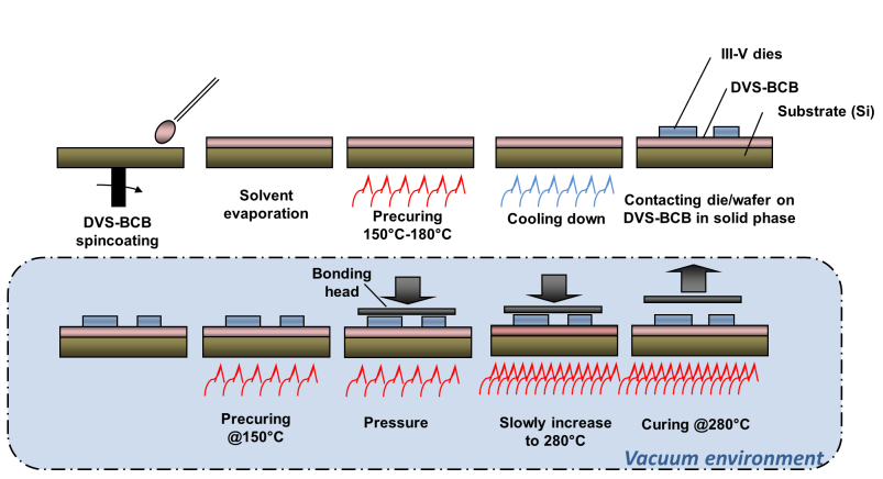
Figure 1: Developed bonding process, referred to as ‘cold bonding’.
We demonstrated a new adhesive wafer bonding process scheme that involves partial curing of the DVS-BCB prior to bonding and attaching the III-V substrate at room temperature prior to curing in a vacuum atmosphere. This ‘cold bonding’ method significantly simplifies the bonding preparation for machine-based bonding both for die and wafer-scale bonding (Figure 1). This approach shows high yield for ultra-thin bonding thicknesses below 50 nm, as well as good uniformity of the DVS-BCB layer thickness after wafer bonding over the full wafer area. This process was applied to achieve ultra-thin DVS-BCB bonding layers for the fabrication of several photonic devices, such as III-V/SOI lasers and optical isolators.
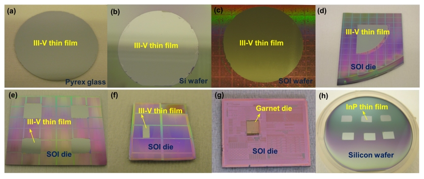
The bonding recipe was originally developed for ultra-thin DVS-BCB bonding layers, suitable for the fabrication of photonic devices, specifically hybrid III-V/Si lasers. Several bonding experiments were performed to evaluate the bonding quality and the DVS-BCB thickness uniformity after wafer bonding. The experimental results wafer-to-wafer, die-to-wafer and multiple die-to-wafer bonding are presented in Figures 2 (a-h). A uniform DVS-BCB thickness for different points distributed over the bonded surface is obtained, with an average bonding layer thickness of 29nm, varying by +/- 3 nm over 2 inch wafer bonding area [1].
Figure 2: A full wafer 300nm InP membrane bonded on a Pyrex glass wafer (a), a 100 mm silicon wafer (b) and a quasi-planarized SOI wafer (c) epitaxial quarter III-V wafer bonded on quasi-planarized SOI (d) after substrate removal; four epitaxial 0.3cm2 III-V dies bonded (e) 1.3mm by 4mm die transferred (f) on a quasi-planarized SOI after the substrate removal process; (f) 0.04cm2 garnet (magneto-optic material) bonded on SOI (g) 6 InP-membranes (with an individual die
Commercial silicon photonics and CMOS production is carried out on wafer diameters of 200 mm and above, while III-V substrates used in photonics applications have typical diameters of less than 100 mm, indicating that wafer-to-wafer bonding will often not be the preferred approach. Moreover, bonding of large III-V areas would result in a waste of material in chip areas were the transferred material is not needed. Therefore, a cost-effective approach in heterogeneous integration requires III-V material or other optical materials to be bonded in small areas of the SOI photonic wafer. We focus on a multiple die-to-wafer bonding process where III-V dies would be bonded to a SOI die or a full SOI wafer. Since the presented method uses contacting of the dies at room temperature, individual dies can easily be pick-and-placed onto a silicon target wafer. They can be aligned with an accuracy of 500μm without any extra tools or can be placed more accurately using a flip-chip machine. The results are shown in Figures. 2 (e-f). In particular situations there is a need for bonding different types of III-V dies on a single SOI die or wafer (e.g. a die containing laser epitaxy and a die containing photodetector epitaxy). This typically results in dies of different height and size to be bonded, which is difficult to achieve using the classical bonding recipe. Here we show that by applying the new bonding recipe, in combination with a graphite foil between the dies and the bonding head, four-die bonding using two different epitaxial layer stacks (with about 50 μm difference in substrate thickness) can be achieved. The graphite foil is used to compensate for these thickness variations in order to distribute the pressure evenly over all dies during the bonding, as is illustrated in Figure 3.
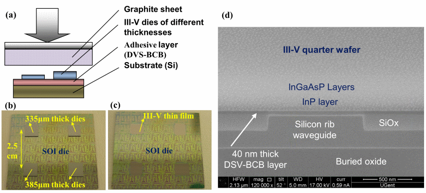
Figure 3: Four-die bonding on planarized SOI with different substrate thickness, using a graphite foil to compensate for die-thickness variations: (a) schematic; (b) before substrate removal; (c) after substrate removal; (d) SEM image
Other people involved: PublicationsInternational Journals
-
N. Poulvellarie, U.D. Dave, K. Alexander, C. Ciret, M. Billet, C. Mas Arabi, F. Raineri, S. Combrie, A. De Rossi, G. Roelkens, S-P. Gorza, B. Kuyken, F. Leo,
Second Harmonic Generation Enabled by Longitudinal Electric Field Components in Photonic Wire Waveguides, Physical Review A, p.023521 (6 pages) doi:10.1103/PhysRevA.102.023521 (2020)
 . .
International Conferences
-
S. Keyvaninia, M. Muneeb, S. Stankovic, S. Ghosh, M. Tassaert, D. Van Thourhout, G. Roelkens,
DVS-BCB Adhesive Bonding for Silicon Photonics, Conference on Wafer Bonding for Microsystems 3D- and Wafer Level Integration (WaferBond ‘13) (invited), Sweden, (2013) .
Back to overview
|